Semiconductor, polished silicon wafer, thin silicon wafer, wafer IC
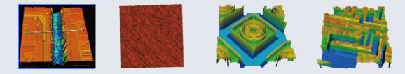
3C electronics, sapphire glass roughness, metal shell mold defects, glass screen height difference
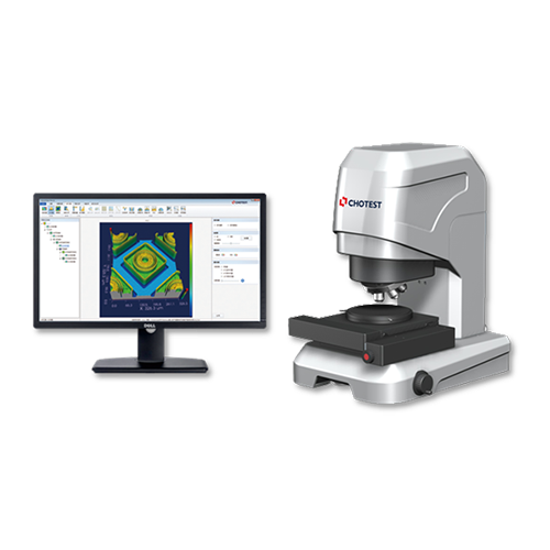
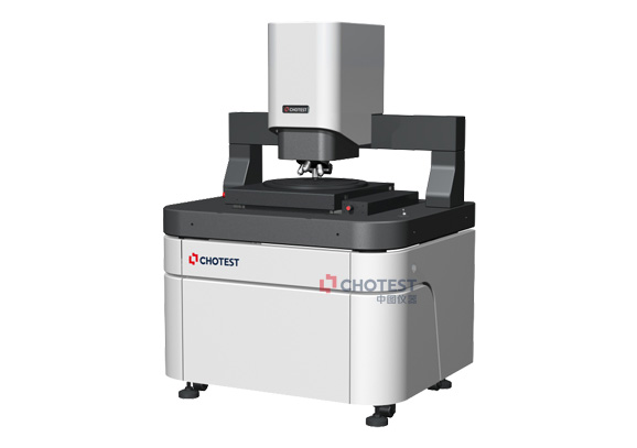
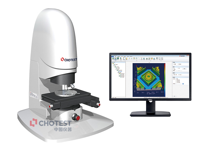
| Model No. | SuperView WX100 | |
| Light Source | White LED | |
| Video System | 1024×1024 | |
| Objective Lens | 10X(2.5X,5X,20X,100X optional) | |
| F.O.V | 0.98×0.98mm(10X) | |
| Lens Turret | Single hole / 3 holes manual | |
| Size | 230×200×380mm | |
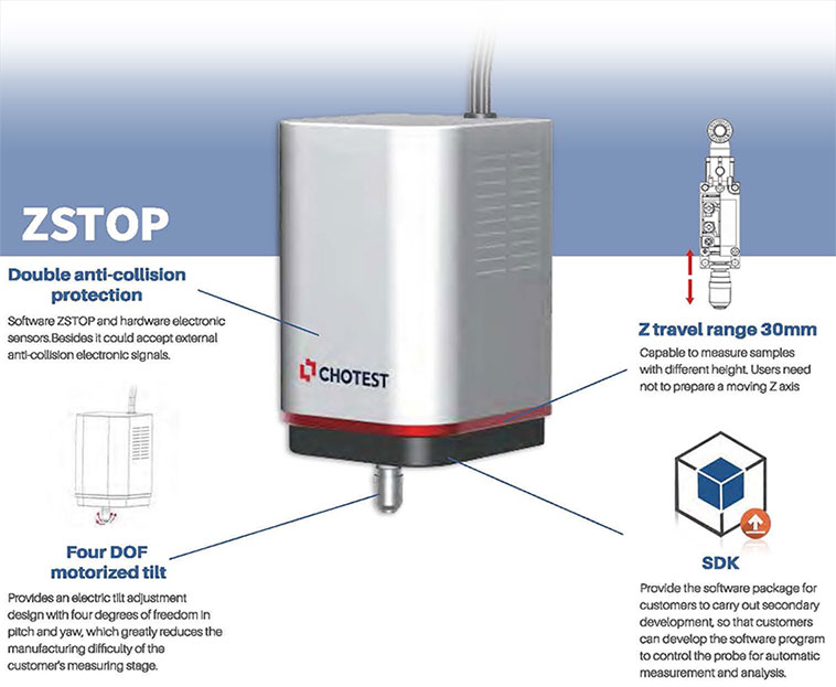
| Tilt | ±2° Motorized | |
| Z Travel Range | 30mm | |
| Z Scanning Range | 10mm(Depend on Lens) | |
| Z Resolution | 0.1nm | |
| Roughness RMS Repeatability*1 | 0.01nm | |
|
Step Height Measurement |
Accuracy*2 | 0.5% |
| Repeatability*2 | 0.1% 1σ | |
|
Note: *1 Measure Sa 0.2nm silicon wafer in a laboratory environment according to the ISO 25178. *2 Measure standard 5μm steps height block in a laboratory environment according to the ISO 10610-1:2009 |
||