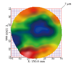
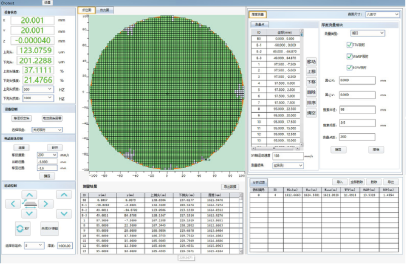
Measurement results of wafer thickness and warpage
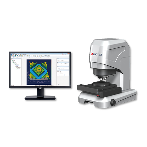
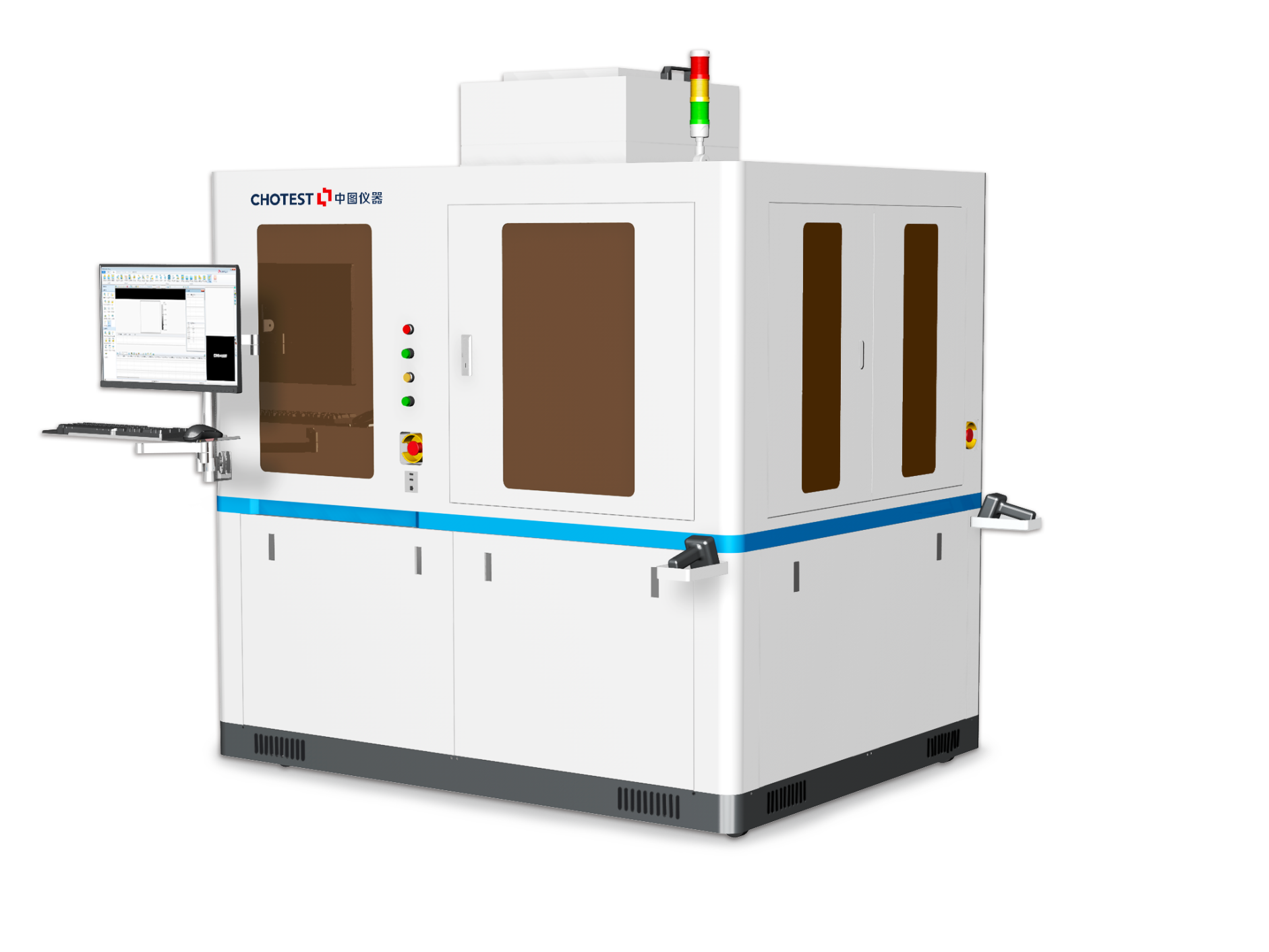
Unpatterned Wafer 3D Inspection System WD4000 series can automatically measure wafer thickness, surface roughness, and micro-nano 3D microtopography at a time. Use white light confocal probes to measure wafer thickness, TTV, LTV, BOW, WARP, line roughness; use white light interferometry probe to scan the Wafer surface to create a 3D profile image of the surface , then analyze the roughness and relevant 2D and 3D parameters according to ISO/ASME/EUR/GBT standards.
The 3D shape based on the upper and lower surfaces of the wafer is reconstructed by non-contact measurement. The powerful measurement and analysis software ensures the stable calculation for the thickness, roughness, total thickness variation(TTV) of the wafer.
|
Thinned silicon wafer
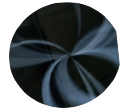
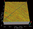
3D image of rough grinding silicon wafer
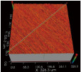 3D image of fine grinding silicon wafer |
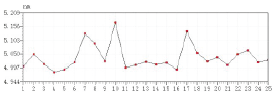
Sa curve of 25 times measurement data for fine grinding wafer 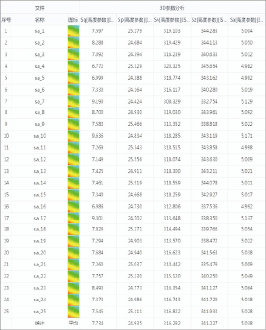
Multi-file analysis of 25 times measurement data for fine grinding wafer
|
| Model No. | WD4100 | WD4200 | |
| Wafer Size | 4", 6" 8" 12" | ||
| Wafer Table | Vacuum chuck | ||
| Loading and Unloading | Manual(Auto robot arm is optional) | ||
| XYZ Travel range | 400mm/400mm/75mm | ||
| Max Moving speed | 500mm/s | ||
| Main Frame | Marble | ||
| Anti-Vibration | Air-floating anti-vibration system | ||
| Loading capacity | <=3kg | ||
| Overall Size | 1500x1500x2000mm | ||
| Weight | About 1500kg | ||
| Compressed Air | 0.6MPa; 60L/min | ||
| Working Environment | Temp, 20°C+1°C/hour, RH 30~80% | ||
| Ambient Vibration | VC-C or better | ||
| Thickness Measurement System | |||
| Material of Object |
Arsenide, nitride, phosphorus, germanium, phosphorurate, lithlum crickets,sapphire, slllcon, silicon carblde. glass, etc |
||
| Sensor | High-precision white light confocal sensors | ||
| Measuring range | 100μm~2000μm | ||
| Scanning Path | Full map area scanning, Union Jack path, free multi-point | ||
| Accuracy | ±0.25μm | ||
| Repeatability( σ) | 0.2μm | ||
| Resolution | 25nm | ||
| Measurement Parameters | Thickness, TTV (Total thickness variation), LTV, BOW, warp, fatness, line roughness | ||
| 3D microtopography Measurement System | |||
| Measurement Principle | ---- | White llght interferometry | |
| Light Source | ---- | White LED | |
| Objective Lens | ---- | 10X(2.5X, 5X, 20X, 50X are optional) | |
| Field of View | ---- | 0.96 * 0.96 mm | |
| Lens Turret | ---- | Single hole | |
| Level Adjustment | ---- | ±2° | |
| Z-axis Scanning Range | ---- | 5 mm | |
| Z-axis Resolution | ---- | 0.1nm | |
| Lateral Resolution | ---- | 0.5~3.7μm | |
| Scanning Speed | ---- | 2.5~5.0μm/s | |
| Characters of Test Object | ---- | Reflectivity 0.05%~100% | |
| Roughness RMS Repeatability*1 | ---- | 0.08nm | |
|
Step Height Measurement*2 |
Accuracy | ---- | 1% |
| Repeatability | ---- | 0.2%1σ | |
| Measurement Parameters | ---- |
Microtopography, line/surface roughness. spatial frequency, etc. |
|
|
*1 Roughness performance is obtained by measuring SQ parametersfor a 0.2nm SA slicon wafer in the laboratory environmant according to ISO 25178. *2 Step height performance is obtained by measuring a standard 4.7μm stage block in the laboratory environment acording to IS0 5436-1:2000. |
|||