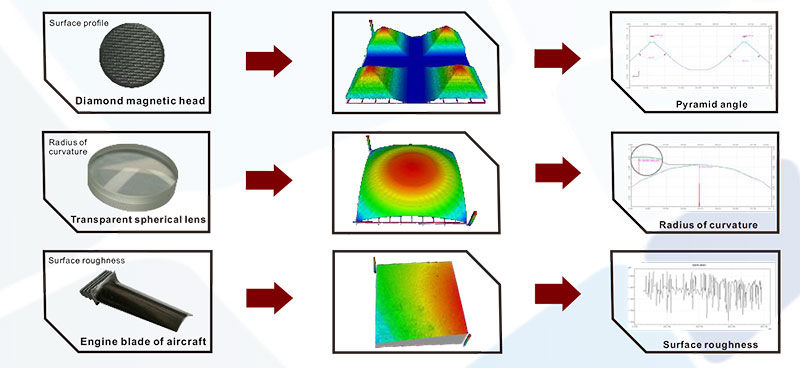
SuperView W5 is mainly used for high-precision measurement of surface roughness and waviness of irregular workpieces. Equipping a 5-axis object table(X/Y/Z axis, tilt & rotation), it can achieve rapid positioning throng imported 3D model. Then the measurement head can automatically scan the specified position and software obtains test data including 2D/3D topography, roughness, waviness, etc.
| Model No. | SuperView W5 | |
| Light Source | White LED | |
| Video System | 1024x1024 | |
| Objective Lens | 10X,20X | |
| Optical Zoom | 0.5X,(0.75X,1X,0.375X) | |
| Field of View | 0.98x0.98mm(10x) | |
|
XY Object Table |
Size | 400x400mm |
| Travel Range | 300x300mm | |
| Load Capacity | 20kg | |
| Control Method | Motorized | |
| Rotary Stage | Tilt | ±90° |
| Rotation | 360° | |
| Load Capacity | 10kg | |
| Control Method | Motorized | |
| Z Axis | Travel Range | 100mm |
| Control Method | Motorized | |
| Z- Stroke Scanning Range | 10mm | |
| Z Resolution | 0.1nm | |
| Roughness RMS Repeatability*1 | 0.005nm | |
|
Step Height Measurement |
Accuracy*2 | 0.5% |
| Repeatability*2 | 0.1% | |
| Working temperature | 0~40°C fluctuation <2℃/h | |
| Working Relative Humidity | ≤70% | |
|
*1 Measure Sa 0.2nm silicon wafer in a laboratory environment according to the ISO 25178. *2 Measure standard 4.7μm steps height block in a laboratory environment according to the ISO 5436-1:2000 |
||
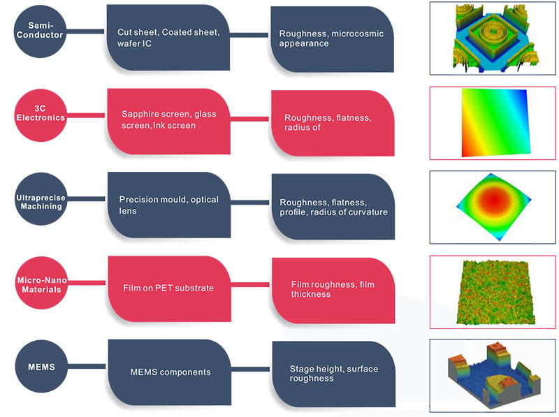
It is used for measurement and analysis of surface roughness and profile of precision components from industries of semi-conductor, 3C Electronics, ultraprecise machining, optical machining, micro-nano materials, micro-electro-mechanical system.

Measurement and analysis for various products, components and materials`surface form and profile characteristics, such as flatness, roughness, waviness, appearance, surface defect, abrasion,corrosion, gap, hole, stage, curvature, deformation, etc.

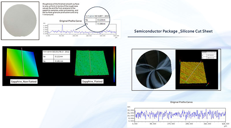
3C Electronics_Sapphire crystal

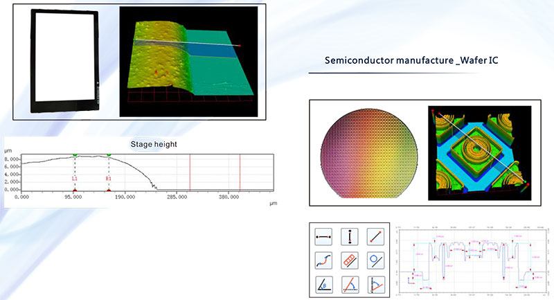
3C Electronics _ Ink screen
