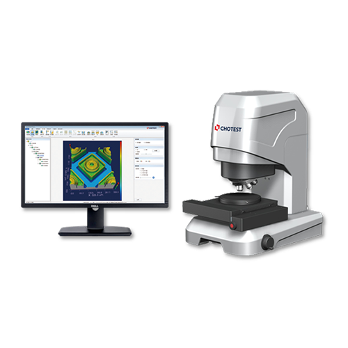
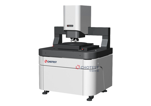
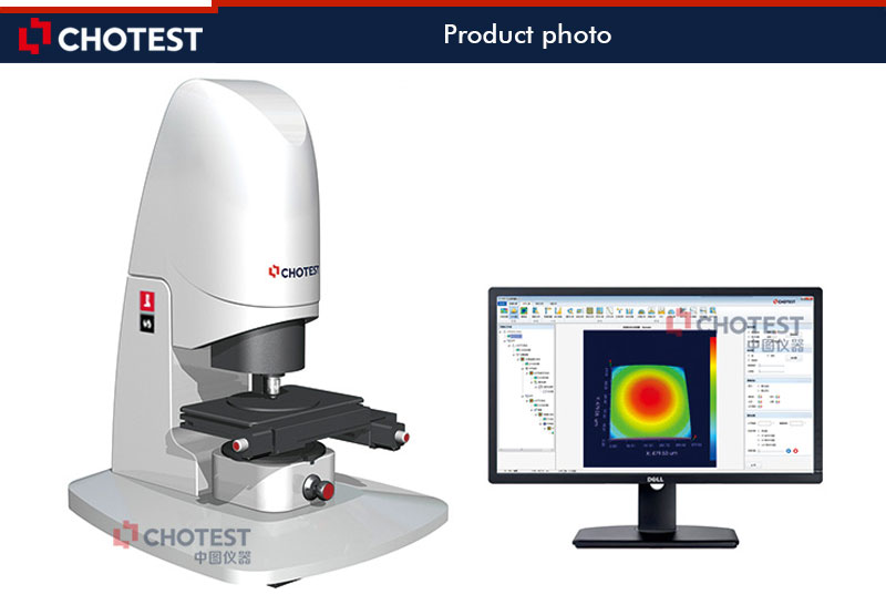
SuperView W1 Optical 3D Surface profilometer is an ideal instrument for sub-Nanometer measurement of various precision parts. Based on the principle of white light interference technology, combined with precision Z-direction scanning module and 3D modeling algorithm, it contactlessly scans the surface of the object then establish a 3D image for the surface. A serial of 2D, 3D parameters reflecting surface quality of the object are obtained after XtremeVision software processes and analyzes the 3D image. The SuperView W1 is a user-friendly precision optical instrument with powerful analysis functions for all kinds of surface form & roughness parameters. With unique light source it could measure various precision parts with both smooth and rough surface.
| Model No. | SuperView W1 | SuperView W1-Pro | SuperView W1-Ultra | SuperView W1-Lite | |
| Light source | White LED | ||||
| Video system | 1024×1024 | ||||
| Objective Lens | Standard: 10X(Optional: 2.5X, 5X, 20X, 50X, 100X) | ||||
| Optical Zoom |
Standard: 0.5X Optional: 0.375X, 0.75X,1X |
Standard: 0.5X Optional: 0.375X, 0.75X |
|||
| Standard Field of View | 0.98×0.98 mm | 1.1x1.1mm | 0.98x0.98mm | ||
| Lens Turret |
Standard: Manual 3 holes turret (Optional: Motorized 5 holes turret) |
Motorized 5 holes turret | |||
| XY Object table | Size | 320×200mm | 300×300mm | 320x200mm | 220x220mm |
| Moving Range | 140×100mm | 200×200mm | 140x100mm | 100x100mm | |
| Loading Capacity | 10kg | ||||
| Control Method | Motorized | ||||
| Tilt(manual) | ±4° | ±3° | |||
| Z Axis focusing | Travel Range | 100mm | 50mm | ||
| Control Method | Motorized | ||||
| Z Stroke Scanning Range | 10mm | ||||
| Surface Form Repeatability*1 | 0.1nm | ||||
| Roughness RMS Repeatability*2 | 0.005nm | 0.01nm | |||
| Step Height Measurementy*3 | Accuracy: 0.3%; Repeatability: 0.08%(1σ) |
Accuracy: 0.7% Repeatability: 0.1%(1σ) |
|||
| Scanning Speed@0.1nm resolution | 1.85μm/s | 1.85μm/s | 8μm/s | 1.65μm/s | |
| Weight | 140KG | 170kg | 140kg | 50kg | |
| Size(L*W*H) | 700x606x920mm | 750x650x950mm | 700x600x900mm | 500x400x700mm | |
| Stage measurement | Temperature | 0°C~30°C, fuctuation <2°C/60min | |||
| Humidity | 5%~95% RH, no condensation | ||||
| Vibration | VC-C or better | ||||
|
Software Noise Evaluation*5 |
3σ≤4nm | ||||
| Compressed Air | 0.6Mpa oil-free, water-free, 6mm diameter of hose | ||||
| Power Supply | AC100~240V, 50/60Hz, 4A, 300W | ||||
| Other | No strong magnetic field, No corrosive gas | ||||
|
Note: *1 Use EPSl mode to measure Sa 0.2nm silicon wafer in the laboratory environment; Single stripe, 80um filter for full field of view *2 Measure Sa 0.2nm silicon wafer in a laboratory environment according to the ISO 25178. *3 Measure standard 5 μm steps height block in a laboratory environment according to the ISO 1060-1:2000 *4 When the software noise evaluation is 4nm≤3σ≤10nm, the Roughness RMS repeatability is revised down to 0.015nm, the Step height measurement accuracy is revised down to 0.7%, and the step height measurement repeatability is revised down to 0.12%; When the software noise evaluation is 3σ>10nm, the environment does not meet the requirement for usage of the equipment, and need to change the site. |
|||||
| Standard | Parameters | |||
| ISO 4287-1997 | P>rincipal section | Roughness | W>aviness | |
| A>mplitude | Pp, Pv ,Pz, Pc, Pt,Pa,Pq,Psk,Pku | Rp, Rv ,Rz, Rc, Rt,Ra,Rq,Rsk,Rku | Wp, Wv ,Wz, Wc, Wt,Wa,Wq,Wsk,Wku | |
| interval | PSm,Pdq | RSm,Rdq | WSm,Wdq | |
| S>ubstance | Pmr,Pdc | Rmr,Rdc,Rmr(Rz/4) | Wmr,Wdc,Wmr(Wz/4) | |
| Peak | PPc | RPc | WPc | |
| ISO 13565 | ISO 13565-2 | Rk,Rpk,Rvk,Mr1,Mr2,A1,A2,Rpk,Rvk | ||
| ISO 12085 | Roughness graph | R,AR,R× ,Nr | ||
| W>aviness> graph | W,AW,W×,Wte | |||
| Other graph | Rke,Rpke,Rvke | |||
| AMSE >B46.1 | 2D | Rt,Rp,Rv,Rz,Rpm,Rma×,Ra,Rq,Rsk,Rku,tp,Htp,Pc,Rda,Rdq,RSm,Wt | ||
| DIN EN ISO 4287-2010 | Original profile | Pa,Pq,Pp,Pv,Pz,Pc,Pt,PSk,PKu,PSm,PPc,Pdq,Pdc,Pmr, | ||
| Roughness | Ra,Rq,Rp,Rv,Rz,Rc,Rt,RSk,RKu,RSm,RPc,Rdq,Rdc,Rmr, | |||
| W>aviness | Wa,Wq,Wp,Wv,Wz,Wc,Wt,WSk,WKu,WSm,WPc,Wdq,Wdc,Wmr | |||
| JIS B0601-2013 | Original profile | Pa,Pq,Pp,Pv,Pz,Pc,Pt,PSk,PKu,PSm,PPc,Pdq,Pdc,Pmr, | ||
| Roughness | Ra,Rq,Rp,Rv,Rz,Rc,Rt,RSk,RKu,RSm,Rdq,Rdc,Rmr | |||
| W>aviness | Wa,Wq,Wp,Wv,Wz,Wc,Wt,WSk,WKu,WSm,WPc,Wdq,Wdc,Wmr | |||
| GBT 3505-2009 | Original profile | Pa,Pq,Pp,Pv,Pz,Pc,Pt,PSk,PKu,PSm,PPc,Pdq,Pdc,Pmr, | ||
| Roughness | Ra,Rq,Rp,Rv,Rz,Rc,Rt,RSk,RKu,RSm,Rdq,Rdc,Rmr | |||
| W>aviness | Wa,Wq,Wp,Wv,Wz,Wc,Wt,WSk,WKu,WSm,WPc,Wdq,Wdc,Wmr | |||
※ Built-in ISO/ASME/EUR/GBT Standards of 2D, 3D parameters:
2D Parameters
| Standard | Parameters | |||
| ISO 4287-1997 | P>rincipal section | Roughness | W>aviness | |
| A>mplitude | Pp, Pv ,Pz, Pc, Pt,Pa,Pq,Psk,Pku | Rp, Rv ,Rz, Rc, Rt,Ra,Rq,Rsk,Rku | Wp, Wv ,Wz, Wc, Wt,Wa,Wq,Wsk,Wku | |
| interval | PSm,Pdq | RSm,Rdq | WSm,Wdq | |
| S>ubstance | Pmr,Pdc | Rmr,Rdc,Rmr(Rz/4) | Wmr,Wdc,Wmr(Wz/4) | |
| Peak | PPc | RPc | WPc | |
| ISO 13565 | ISO 13565-2 | Rk,Rpk,Rvk,Mr1,Mr2,A1,A2,Rpk,Rvk | ||
| ISO 12085 | Roughness graph | R,AR,R× ,Nr | ||
| W>aviness> graph | W,AW,W×,Wte | |||
| Other graph | Rke,Rpke,Rvke | |||
| AMSE >B46.1 | 2D | Rt,Rp,Rv,Rz,Rpm,Rma×,Ra,Rq,Rsk,Rku,tp,Htp,Pc,Rda,Rdq,RSm,Wt | ||
| DIN EN ISO 4287-2010 | Original profile | Pa,Pq,Pp,Pv,Pz,Pc,Pt,PSk,PKu,PSm,PPc,Pdq,Pdc,Pmr, | ||
| Roughness | Ra,Rq,Rp,Rv,Rz,Rc,Rt,RSk,RKu,RSm,RPc,Rdq,Rdc,Rmr, | |||
| W>aviness | Wa,Wq,Wp,Wv,Wz,Wc,Wt,WSk,WKu,WSm,WPc,Wdq,Wdc,Wmr | |||
| JIS B0601-2013 | Original profile | Pa,Pq,Pp,Pv,Pz,Pc,Pt,PSk,PKu,PSm,PPc,Pdq,Pdc,Pmr, | ||
| Roughness | Ra,Rq,Rp,Rv,Rz,Rc,Rt,RSk,RKu,RSm,Rdq,Rdc,Rmr | |||
| W>aviness | Wa,Wq,Wp,Wv,Wz,Wc,Wt,WSk,WKu,WSm,WPc,Wdq,Wdc,Wmr | |||
| GBT 3505-2009 | Original profile | Pa,Pq,Pp,Pv,Pz,Pc,Pt,PSk,PKu,PSm,PPc,Pdq,Pdc,Pmr, | ||
| Roughness | Ra,Rq,Rp,Rv,Rz,Rc,Rt,RSk,RKu,RSm,Rdq,Rdc,Rmr | |||
| W>aviness | Wa,Wq,Wp,Wv,Wz,Wc,Wt,WSk,WKu,WSm,WPc,Wdq,Wdc,Wmr | |||
3D Parameters
| Standard | Parameters | |
| ISO 25178 | Height | Sq,Ssk,Sku,Sp,Sv,Sz,Sa |
| function | Smr,Smc,S×p | |
| Space | Sal,Str,Std | |
| Composite parameters | Sdq,Sdr | |
| Volume | Vm,Vv,Vmp,Vmc,Vvc,Vvv | |
| Form | Spd,Spc,S10z,S5p,S5v,Sda,Sha,Sdv,Shv | |
| Functional | Sk,Spk,Svk,Smr1,Smr2,Spq,Svq,Smq | |
| ISO 12781 | Flatness | FLTt,FLTp,FLTv,FLTq |
| EUR 15178N | Amplitude | Sa,Sq,Sz,Ssk,Sku,Sp,Sv,St |
| Space | Str,Std,Sal | |
| Composite parameters | Sdq,Sds,Ssc,Sdr,Sfd | |
| Area, Volume | Smr,Sdc | |
| Function | Sk,Spk,Svk,Sr1,Sr2,Spq,Svq,Smq | |
| Functional | Sbi,Sci,Svi | |
| EUR 16145 EN | Amplitude | SaSq,Sy,Sz,Ssk,Sku |
| Mixed parameters | Ssc,Sdq | |
| Functional | Sbi,Sci | |
| Space | Sdsrw | |
| Hardness | Hs,Hvol | |
| ASME B46.1 | 3D | St,Sp,Sv,Sq,Sa,Ssk,Sku,SWt |
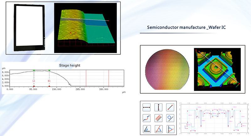
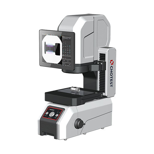
It is used for measurement and analysis of surface roughness and profile of precision components from industries of semi-conductor, 3C Electronics, ultraprecise machining, optical machining, micro-nano materials, micro-electro-mechanical system.
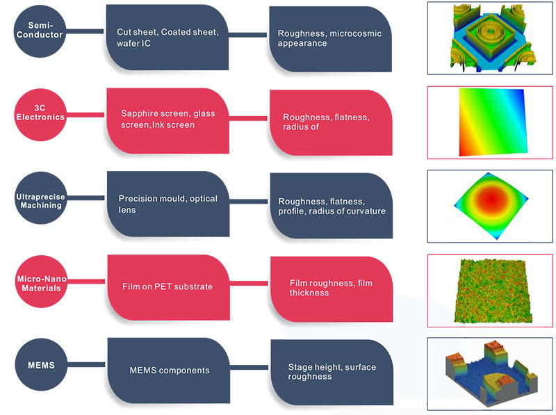
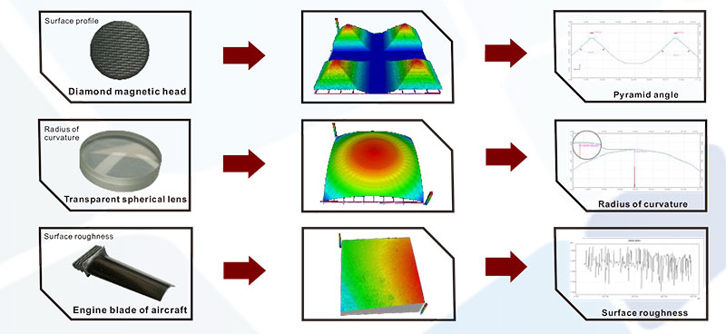
Measurement and analysis for various products, components and materials`surface form and profile characteristics, such as flatness, roughness, waviness, appearance, surface defect, abrasion,corrosion, gap, hole, stage, curvature, deformation, etc.
3C Electronics_Sapphire crystal
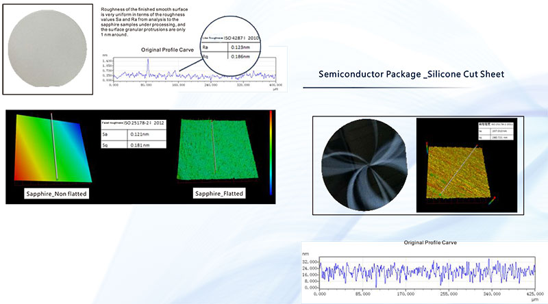
3C Electronics _ Ink screen