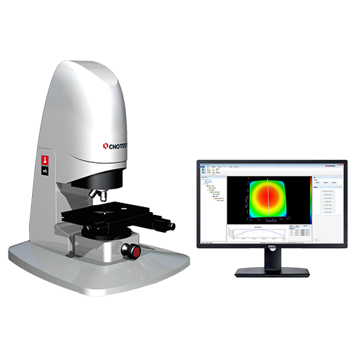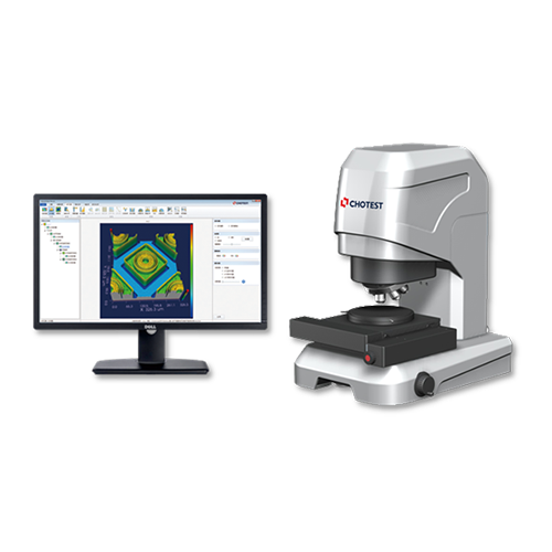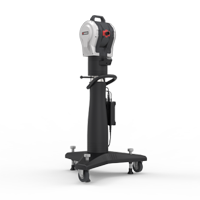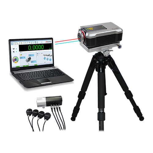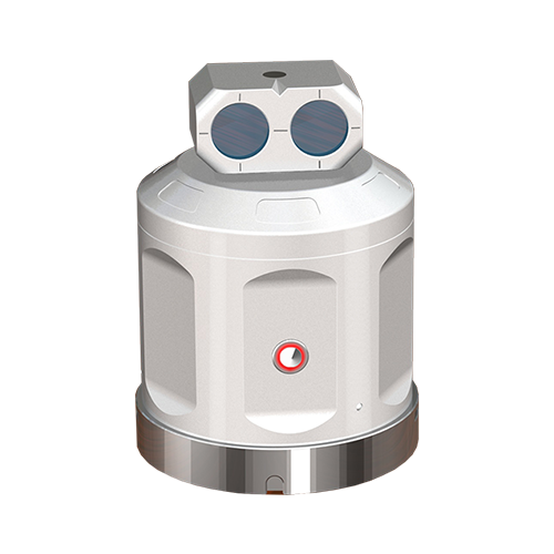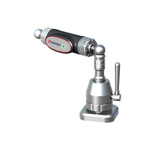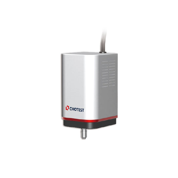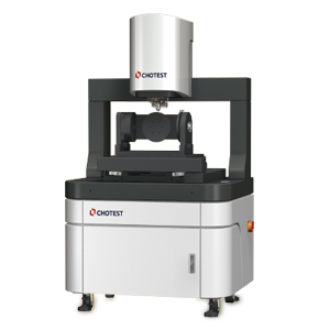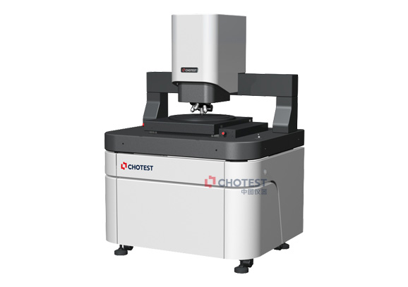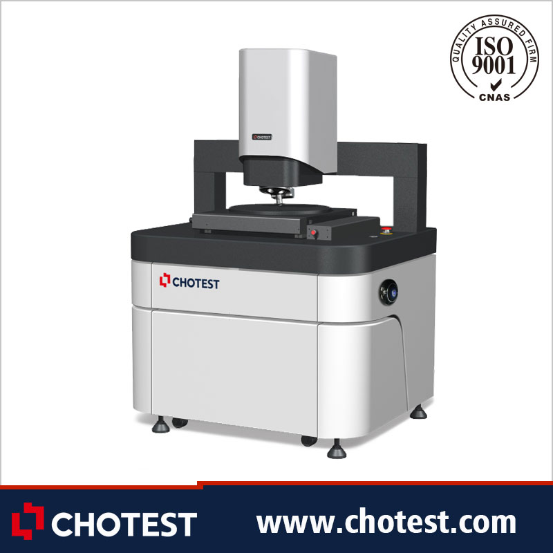
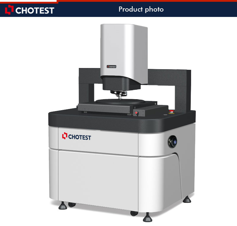
SuperView W2 Optical 3D Surface profilometer is an ideal instrument for sub-Nanometer measurement of various precision parts. Based on the principle of white light interference technology, combined with precision Z-direction scanning module and 3D modeling algorithm, it contactlessly scans the surface of the object then establish a 3D image for the surface. A serial of 2D, 3D parameters reflecting surface quality of the object are obtained after XtremeVision software processes and analyzes the 3D image. The SuperView W3 is a user-friendly precision optical instrument with powerful analysis functions for all kinds of surface form & roughness parameters. With unique light source it could measure various precision parts with both smooth and rough surface.
| Model No. | SuperView W2 | SuperView W2-Ultra | |||
| Light Source | White LED | ||||
| Video System | 1024×1024 | ||||
| Objective Lens | Standard: 10X(Optional: 2.5X, 5X, 20X, 50X, 100X) | ||||
| Optical Zoom | Standard: 0.5X(Optional: 0.375X, 0.75X,1X) | ||||
| Standard Field of View | 0.98×0.98mm | 1.1*1.1mm | |||
| Lens Turret | Motorized 5 holes turret | ||||
| XY Object Table | Size | Φ312mm | |||
| Moving Range | 200×200mm | ||||
| Loading Capacity | 20kg | ||||
| Control Mode | Motorized | ||||
| Tilt | ±2°(Motorized) | ||||
| Z Axis Focusing | Travel Range | 100mm | |||
| Control Mode | Motorized | ||||
| Z Stroke Scanning Range | 10mm | ||||
| Surface Topography Repeatability*1 | 0.1nm | ||||
| Roughness RMS Repeatability*2 | 0.005nm | ||||
| Step Height Measurementy*3 | Accuracy: 0.3%; Repeatability: 0.08%(1σ) | ||||
| Scanning Speed@0.1nm Resolution | 5μm/s | 16μm/s | |||
| Weight | 535kg | ||||
| Size(LxWxH)mm | 800x700x1520 | ||||
| Working Environment | Temperature | 0°C~30°C, fuctuation <2°C/60min | |||
| Humidity | 5%~75% RH, no condensation | ||||
| Vibration | VC-C or better | ||||
| Software Noise Evaluation*4 | 3σ≤4nm | ||||
| Compressed Air | 0.6Mpa oil-free, water-free, 6mm diameter of hose | ||||
| Power Supply | AC100~240V, 50/60Hz, 300W | ||||
| Other | No strong magnetic field, No corrosive gas | ||||
|
*1 Use EPSl mode to measure Sa 0.2nm silicon wafer in the laboratory environment; Single stripe, 80um filter for full field of view *2 Measure Sa 0.2nm silicon wafer in a laboratory environment according to the ISO 25178. *3 Measure standard 5μm steps height block in a laboratory environment according to the ISO 5436-1:2000 *5 When the software noise evaluation is 4nm≤3σ≤10nm, the Roughness RMS repeatability is revised down to 0.015nm, the Step height measurement accuracy is revised down to 0.7%, and the step height measurement repeatability is revised down to 0.12%; When the software noise evaluation is 3σ>10nm, the environment does not meet the requirement for usage of the equipment, and need to change the site. |
|||||
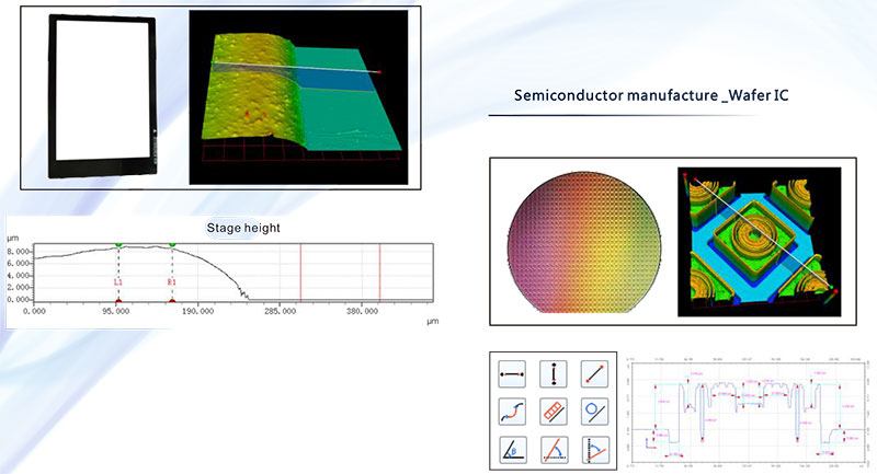
It is used for measurement and analysis of surface roughness and profile of precision components from industries of semi-conductor, 3C Electronics, ultraprecise machining, optical machining, micro-nano materials, micro-electro-mechanical system.
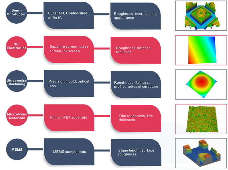
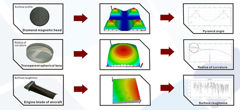
Measurement and analysis for various products, components and materials`surface form and profile characteristics, such as flatness, roughness, waviness, appearance, surface defect, abrasion,corrosion, gap, hole, stage, curvature, deformation, etc.
3C Electronics_Sapphire crystal
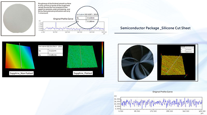
3C Electronics _ Ink screen